What is CTI?#
Charge Transfer Inefficiency, or CTI for short, is an effect that occurs when acquiring imaging data from Charge Coupled Devices (CCDs).
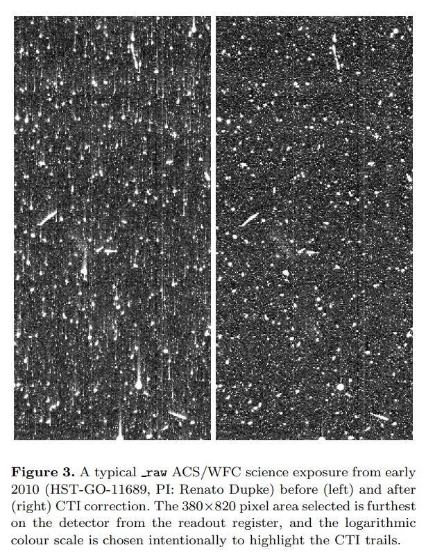
Lets take a look at a extract of data taken from the Advanced Camera for Surveys (ACS) instrument on board the
Hubble Space Telescope (this figure is taken from Massey et al 2009 https://arxiv.org/abs/1009.4335):
Trailing#
On the left hand side of the figure, we can see CTI is action. Upwards from all the bright sources of light (which are of galaxies, stars and cosmic rays) we see a trailing or smearing effect. This is not a genuine signal emitted by each galaxy or star, but is instead induced during data acquisition.
On the right hand side of the figure, we can see that when a CTI correction is applied this trailing effect is entirely removed from the data.
This trailing effect is the characteristic signal of Charge Transfer Inefficiency, and removing it is pretty much what PyAutoCTI is all about!
CCD Clocking#
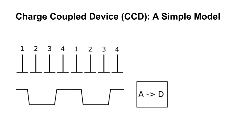
To understand at a physical level what CTI is, we first need to understand how a CCD acquires imaging data. This is a massive over simplification, but in order to understand CTI this process can be simplified into 4 steps:
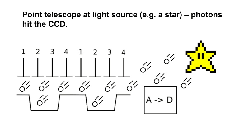
1) Point a telescope (e.g. the Hubble Space Telescope) towards light sources (e.g. stars, galaxies, etc.) whose photons are collected via the telescope mirror and hit the CCD.
2) These photons interact with a silicon lattice inside the CCD and via the photoelectric effect are converted into (photo-)electrons. These electrons make-up the signal that we observe (e.g. the galaxies, stars and cosmic rays in the image above).
3) Left to their own accord, these electrons would move freely over the CCD and we would lose our image of the galaxies and stars. Therefore, an electrostatic potential runs over the CCD, which applies voltage difference that hold electrons in place wherever they interacted with the silicon lattice. The electrons therefore maintain their 2D spatial locations, corresponding to the 2D pixels we see in the image above.
4) We finally convert this analogue signal of electrons into a digital image. By varying the voltages of the electrostatic potential we can move electrons across the CCD, towards the ‘read-out electronics’ which perform this analogue to digital conversion. The end result of this process is a 2D digital image, like the one shown above.
The animation below shows this process in action:
CTI#
Now we know how a CCD works, we can understand what CTI is.
During the CCD clocking process, there are defections and imperfections in the CCD’s silicon lattice, called ‘traps’. These traps capture electrons and hold them for a certain amount of time. Depending on the length of time they hold the electron, one of two things can happen:
The release time is shorter than the clocking speed of the CCD, such that the electron is released with its original group of electrons that are collectively held together in the same electrostatic potential (e.g. they all correspond to the same pixel in the image). In this case there is no trailing or smearing.
The release time is longer than the clocking speed of the CCD. In this case, the electron’s original group of electrons have already moved on, well away from the electron. This means that when the electron is released, it joins a different group of electrons in a preceeeding electrostatic potential (e.g. the electrons appears in a different image pixel). Clearly, this is responsible for the trailing effect we’ve seen in the images above!
The animation below shows the CCD clocking process, but now includes one of these traps:
Charge Transfer#
We can now understand why CTI is called Charge Transfer Inefficiency: it is simply the inefficient transfer of charge (e.g.a flow of electrons)!